40 rf front end block diagram
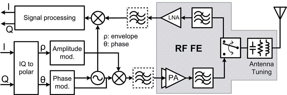
(a) Simplified block diagram of the RF front-end. (b ... (a) Simplified block diagram of the RF front-end. (b) Frequency plan. Source publication +9 A 900-MHz transceiver chipset for two-way paging applications Article Full-text available Jan 1999 Sergio... A Multi-Cell Front-End for Longer Battery Life 11.03.2022 · Renesas released a BMS analog front end, dubbed the “stacked battery front end,” in November. This analog component is a Li-ion battery manager IC that can handle up to 14 series-connected cells. The RAA489204 has all of the features that a battery management system needs, including accurate cell voltage and temperature monitoring, cell balancing, and …
RF Agile Transceiver Data Sheet AD9363 - Analog Devices FUNCTIONAL BLOCK DIAGRAM igure 1. GENERAL DESCRIPTION The AD9363 is a high performance, highly integrated RF agile transceiver designed for use in 3G and 4G femtocell applications. Its programmability a nd wideband capability make it ideal for a broad rang e of transceiver applications. Th e device combines an RF front end with a flexible mixed-signal …
Rf front end block diagram
Solved [50 points] A dual-band radio handset has an RF ... [50 points] a dual-band radio handset has an rf receiver front-end block diagram such as the one shown below if mixer i-channel antenna receiver front-end mixerl buffer lowpass filters duplexer rf ilter rflna image reject filteramp amp filter lo 5 6 q-channel each stage in this receiver is given a number and the table below contains the … Developing a UHF RFID Reader RF Front End with an Analog ... A UHF RFID reader RF front end using an AD9361 block diagram. The AD9361 transmitter monitor path gain distribution is comprised of two gains: front-end gain (transmitter monitor gain) and receive low-pass filter gain (G BBF ). The transmitter monitor gain could be set to 0 dB, 6 dB, or 9.5 dB. G BBF could be set from 0 dB to 24 dB with 1 dB step. PDF RF Front-End Challenges for Joint Communication and Radar ... RF Front-End Challenges for Joint Communication and Radar Sensing ... padmanava.sen, andre.nollbarreto, gerhard.fettweis@barkhauseninstitut.org Abstract—In this paper, radio-frequency (RF) hardware challenges for joint communication and radar sensing (JC&S) applications are studied. ... shows the block diagram of a typical Fig. 2: Chirp-based ...
Rf front end block diagram. PDF AN4855 ISSUE 2.0 October 1999 - Massachusetts Institute of ... A Block Diagram of the GPS Orion receiver design appears in Figure 1. The GPS Orion receiver board com-prises the following components:- GP2015 ultra-miniature GPS RF front-end IC, including:-- RF input bandpass filter and +5V DC active antenna supply DW9255 GPS band-definition SAW filter, supplied by Dynex Semiconductor ( ). Modeling RF Front End in Radar System Simulation - MATLAB ... Modeling RF Front End in Radar System Simulation. In a radar system, the RF front end often plays an important role in defining the system performance. For example, because the RF front end is the first section in the receiver chain, the design of its low noise amplifier is critical to achieving the desired signal to noise ratio (SNR). › media › enDual-Channel, 3.3 GHz to 4.0 GHz, 20 W Receiver Front End ... The ADRF5515 is a dual-channel, integrated RF, front-end, multichip module designed for time division duplexing (TDD) applications. The device operates from 3.3 GHz to 4.0 GHz. The ADRF5515 is configured in dual channels with a cascading, two-stage, LNA and a high power silicon SPDT switch. In high gain mode, the cascaded two-stage LNA and switch PDF RF Front End Module Architectures for 5G A typical RFFE for 5G is presented in Fig. 1 and the transition from 3G/4G FEMs to 5G FEMs poses the following challenges: Fig. 1. 4G/5G RF front end diagram. • Improve the power efficiency for mmWave FR2 radios; most probably FR2 will be used mainly for downlink in mobile applications [10, 11].
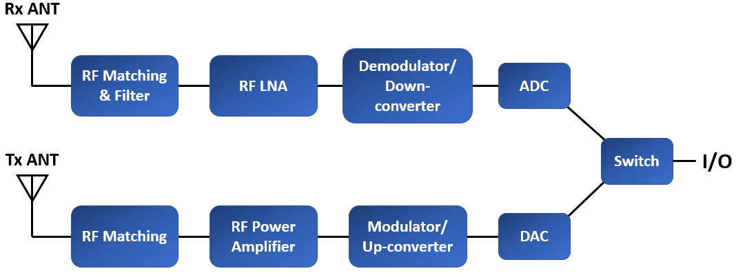
RF Front End Design: Specifications and Component ... The RF front end contains a number of components that work together to ensure signal integrity throughout the signal's bandwidth. This includes preparing a signal for transmission, as well as receiving and demodulating a signal received on the Rx side. The functional block diagram below shows the general topology of an RF front end. Top Design Tips for the Automotive RF Front End - Qorvo Integrating more functions into a front-end module (FEM) or filter modules helps to simplify the RF design, as shown in the next block diagram. (A bonus? Integrating the right filter technology inherently helps manage the coexistence issues we discussed earlier, as well as thermal challenges.) Complete Stand-Alone GPS Receiver Solutio - Maxim Integrated Figure 1. GPS RF front-end block diagram. Table 1. RF Portion System Building Block Table 2. System Cascaded Performance For Larger Image Figure 2. GPS RF portion schematic for MAX2742. Complete Stand-Alone GPS Receiver Solution There are more building blocks to construct a complete GPS receiver, other than just the RF plus baseband IC. GPS front-end block diagram - Electronic Products They have very low noise figures and superior linearity performance, so they help improve overall sensitivity which in turn leads to faster TTFF and better tracking. The devices restore sensitivity, provide greater immunity against out-of-band cellular signals, reduce filtering requirements, and lower overall cost. Download Full Block Diagram Below
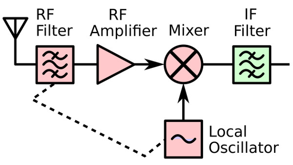
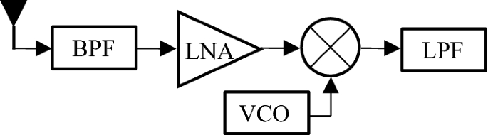
RF generic front-end block diagram - Electronic Products RF generic front-end block diagram Posted on January 6, 2014 by Electronic Products In virtually every wireless application from mobile or networking infrastructure (W-LAN / ISM / RFID), through fixed wireless and industrial applications including e-metering there is always a demand to improve basestation performance. Basestations Superheterodyne receiver - Wikipedia The diagram at right shows the block diagram of a typical single-conversion superheterodyne receiver. The diagram has blocks that are common to superheterodyne receivers, with only the RF amplifier being optional. The antenna collects the radio signal. The tuned RF stage with optional RF amplifier provides some initial selectivity; it is necessary to suppress the image … Block 1: RF Front End - Academics | Bradley University Figure 3: Sub-Level Block Diagram Block 1: RF Front End. A RF signal is input into the RF front end as shown in Figure 4. In lab, a signal generator produces the RF signal, but in application, an antenna would be used to receive the signal. The signal is amplified in a low-noise amplifier (LNA) to increase the power of the input signal. › media › enRF Agile Transceiver Data Sheet AD9361 - Analog Devices The AD9361 is a high performance, highly integrated radio frequency (RF) Agile Transceiver™ designed for use in 3G and 4G base station applications. Its programmability and wideband capability make it ideal for a broad range of transceiver applications. The device combines a RF front end with a flexible mixed-signal
Block Diagram Print - Qorvo
RF Transceiver : Block Diagram, Working, Specifications ... RF Transceiver Module - Block Diagram & Its Working. Generally, an RF module is a small size electronic device, that is used to transmit or receive radio signals between two devices. The main application of the RF module is an embedded system to communicate with another device wirelessly. This communication may be accomplished through radio ...
Testing Wi-Fi 6E performance
RF front-end - Infineon Technologies RF front-end solutions from Infineon. As a leading provider with over 60 years experience developing RF front-end solutions, Infineon offers you a broad product portfolio of high performance RF front-end components. Choose our innovative solutions and benefit from speedy, reliably delivery as well as our in-depth system knowledge and on-site ...
Figure 1 from A 0.1–2 GHz CMOS RF front-end for Software ...
PDF Mobile Phone RF Front End Integration Roadmap Front End Block Diagram CA the Three Bands LB -699 to 960 MHz MB -1428 to 2170 MHz HB -2300 to 2690 MHz J. Young "arrier Aggregation, Quantifying Front End Losses," IWPC Chicago Meeting Sept. 16, 2014 2, 3, 4G Module LB GGE MB GGE B1 B4 B25 B3 B8 B20 B26 B12 PA Bias and Control MIPI Interface Switch Bias and Control Load
![Solved [50 points] A dual-band radio handset has an RF ...](https://d2vlcm61l7u1fs.cloudfront.net/media%2F546%2F546a358f-4da7-45df-be3d-729bc15864f3%2FphpVrp8LR.png)
Solved [50 points] A dual-band radio handset has an RF ...
Superheterodyne Receiver: Block Diagram » Electronics Notes RF tuning & amplification: This RF stage within the overall block diagram for the receiver provides initial tuning to remove the image signal. It also provides some amplification. There are many different approaches used within the RF circuit design for this block dependent its application. The electronic circuit design presents some challenges.

Digital Front - an overview | ScienceDirect Topics
RF front end - Wikipedia Block diagram of a superheterodyne receiver. The RF front end consists of the components on the left colored red. In a radio receiver circuit, the RF front end, short for radio frequency front end, is a generic term for all the circuitry between a receiver's antenna input up to and including the mixer stage.
Not Quite 101 Uses For An Analog UHF TV Tuner | Hackaday
Developing a UHF RFID Reader RF Front End - Semiconductor ... A UHF RFID reader RF front end using an AD9361 block diagram. The AD9361 transmitter monitor path gain distribution is comprised of two gains: front-end gain (transmitter monitor gain) and receive low-pass filter gain (GBBF). The transmitter monitor gain could be set to 0 dB, 6 dB, or 9.5 dB. GBBF could be set from 0 dB to 24 dB with 1 dB step.
Wireless Transceivers RF CMOS Front Ends - AnySilicon
Block Diagrams for RF and Microwave Systems - Pasternack Pasternack's library RF and microwave block diagram are designed to provide engineers and designers with examples of common RF systems schematics while illustrating the RF products and where they fit into the system's design.
IMS 5G Summit: Design challenges remain (part 1) - 5G ...
PDF Electronic Warfare Digital Radar Receiver - Bradley Figure 3: Sub-Level Block Diagram Block 1: RF Front End A RF signal is input into the RF front end as shown in Figure 4. In lab, a signal generator produces the RF signal, but in application, an antenna would be used to receive the signal. The signal is amplified in a low-noise amplifier (LNA) to increase the power of the input signal.
ShareTechnote
PDF Design of Reconfigurable Radio Front-Ends A multi-band transceiver with wideband, fully-integrated RF front-end connects directly to the antenna with no dis- crete, xed-band components, while an e cient, low power spectrum sensing receiver pro- vides real-time environmental knowledge to enable self-adaptation and dynamic recon gura- bility. 1.1 Scope of Work
EMB2538PA IEEE 802.15.4/Zigbee - Radio Frequency Module Block ...
› articles › test-methodsWhat is a Vector Network Analyzer, VNA - Electronics Notes The diagram shows a high level block diagram of an RF network analyzer showing the main circuit blocks: Processor and display: This area of the RF network analyzer acts as the human machine interface, displaying the results in the required fashion - it is possible to display the results of the network analysis in a variety of formats including ...

Developing a UHF RFID Reader RF Front End with an Analog ...
PDF LTE RF Front-End Architecture 2 LTE RF Front-End Design Challenges ... As shown in the simplified diagram below, the key front end components are power amplifiers (PA) and transmit/receive path or duplex filters and switches for band selection or antenna switch module. Figure 1. Simplified Front -End Block Diagram . From UMTS to LTE and beyond, the RF component technologies ...

ADI's RF front-end series supports compact 5g large-scale ...
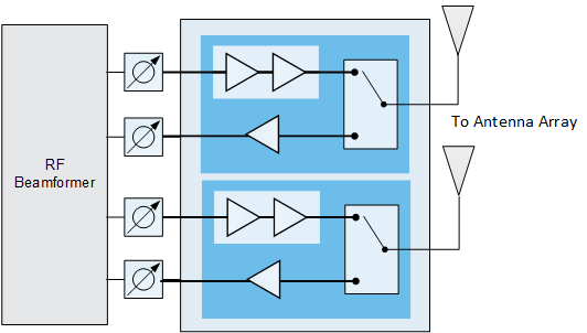
5G Cell Phone Block Diagram - RF Wireless World The figure-2 depicts basic block diagram of 5G cell phone architecture. As shown the architecture include baseband part, digital RF interface such as DigRF, ADC/DAC and RF Transceiver. The basic components are same in the 5G phone except antenna array is used instead of one antenna to support massive MIMO and beamforming.
Performance Analysis of Modular RF Front End for RF ...
Qualcomm 315 5G IoT Modem | Qualcomm Enabling up to 50% smaller modules than existing 5G modules that involves a reduced chipset footprint with highly integrated RF front-end. Qualcomm 315 is purposely designed to provide a pin-to-pin compatible solution for current LTE legacy modules and provides for a seamless transition from LTE to 5G. Legacy modules can upgrade their solutions with no changes …

ADI's RF Platform Hunkers Down on Phase Determinism for ...
VME Bus Description, Pinout and VME Standards information VME Bus Description The VME bus is a scalable backplane bus interface. VME Cards may be produced which respond to the following Address widths or Data widths: A01 - A15, A01 - A23, A01 - A31, or A01 - A40 D00 - D07, D00 - D15, D00 - D23, D00 - D31, or D00 - D63 (undefined before Rev. C). The tables below detail the required control signals to produce the different bus …
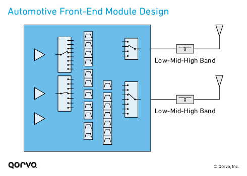
Top Design Tips for the Automotive RF Front End - Qorvo
PDF 2.4-GHz RF FRONT END - TI 2.4-GHz RF FRONT END Check for Samples: CC2595 1FEATURES• Less Than 1-μA Current Consumption in • Low Cost and Small Package Power Down Mode • Very Few External Components • Low Transmit Current Consumption • 2.0-V to 3.6-V Operation • 98 mA at 3 V for +20.7 dBm Out (PAE = 40%) • RoHS Compliant 3- x 3-mm QFN-16 Package DESCRIPTION
RF front-end block diagram | Download Scientific Diagram
Tsmc rf process - greetsieler-grachten-stern.de The RF receiver front-end design consists of low noise amplifier, low power mixer and bandpass Gm-C loop filter. On this basis, not only 5nm, the company is also continuously expanding in the 6nm process. 2020. At TSMC, we bring together the most creative minds in science and technology to provide the best foundry services possible, and drive innovation in fields that …

Hydra – RF Front End – Professor Robert W. Heath Jr.
PDF Multi-band Sub-GHz RF Front End - Mouser Electronics Figure A: SX1250 Block Diagram General Description The SX1250 is a sub-GHz RF Front End device designed to work along with Semtech's SX1302 baseband engine, to design a high-performing LoRa® or LoRaWAN gateway. It covers any frequency band below 1 GHz, making it the perfect candidate to support any license-free band used in today's IOT use cases.
Your RF Amplifier Selection Guide - Blog - Octopart
Block diagram of the designed RF tuner. | Download ... The block dia- gram of the tuner is as shown in Fig. 2. Except for the front-end, all circuit blocks are shared for dual-band operation to save chip area. The signal received from the UHF-or L-band...

Figure 1 from Automotive multi-standard RF front-end for GSM ...
Detection and Measurement of Radar Signals: A Tutorial In this case, even with 50 dB of RF attenuation invoked in the instrument’s front end, an additional 10 dB of external RF attenuation is required between the directional coupler and the measurement device input. B.2 Radiated Coupling to a Radar Transmitter All the caveats regarding maximum allowable input power levels and optimal linear response

Sensors | Free Full-Text | A Low-Band Multi-Gain LNA Design ...
Home | Guerrilla RF 5G TDD mMIMO Block Diagram. 5G FDD mMIMO Block Diagram. 5G mmW Block Diagram. 5G/4G Small Cell Block Diagram. 4G Femtocell Block Diagram . Repeaters/Boosters/DAS. Repeater/DAS Block Diagram. Automotive. Composite Block Diagram. GPS/GNSS Front End Solutions. SHARK FIN - SDARS FRONT END. V2X Compensator. Company. About Us. …

Manifold Multiplexer | IntechOpen
PDF GPS front-end components - Infineon Technologies Below is a general block diagram for GPS functionality in a device. From the antenna looking into GPS receiver, the ESD device protects the RF front-end against ESD hazards coming from ANT when it makes contact with the external environ-ment. In modern wireless handheld systems, 8 kV contact dis-
Modular Design of RF Front End for a Nanosatellite ...
SX1272 | Long Range, Low Power RF Transceiver 860-1000MHz ... Bullet-proof front end: IIP3 = -12.5dBm; 89dB blocking immunity; Low RX current of 10mA, 100nA register retention ; Fully integrated synthesizer with a resolution of 61Hz; FSK, GFSK, MSK, GMSK, LoRa and OOK modulation; Built-in bit synchronizer for clock recovery; Preamble detection; 127dB Dynamic Range RSSI; Automatic RF Sense and CAD with ultra-fast AFC; …

RF SOI Solutions as a Platform for Wireless Front-end ...
ADI's RF Front-End Family Enables Compact 5G Massive MIMO ... An ADRF5545A/ADRF5547/ADRF5549 application block diagram for a M-MIMO RF front-end design is shown in Figure 1. The device has channels that incorporate a high power switch followed by a two stage LNA. During receive mode operation of the transceiver, the switch routes the input signal to the LNA input.
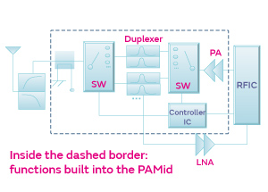
PAMid | Products & Markets | Murata's technical Magazine ...
1 KW SSPA for 1.8-54 MHz - W6PQL Details on the construction and performance of the RF deck are at the end of this article. The rear panel has all the usual connections; input/output, power supply, attenuator configuration jumpers, ALC and PTT. In addition to these is a band select interface connector, which allows the driving radio to control the band switch function in the amplifier. When used, the front panel band …

RF Front End Design: Specifications and Component Selection ...
PDF RF Front-End Challenges for Joint Communication and Radar ... RF Front-End Challenges for Joint Communication and Radar Sensing ... padmanava.sen, andre.nollbarreto, gerhard.fettweis@barkhauseninstitut.org Abstract—In this paper, radio-frequency (RF) hardware challenges for joint communication and radar sensing (JC&S) applications are studied. ... shows the block diagram of a typical Fig. 2: Chirp-based ...

SKY66113-11 RF Front-End Module - Skyworks Solutions Inc ...
Developing a UHF RFID Reader RF Front End with an Analog ... A UHF RFID reader RF front end using an AD9361 block diagram. The AD9361 transmitter monitor path gain distribution is comprised of two gains: front-end gain (transmitter monitor gain) and receive low-pass filter gain (G BBF ). The transmitter monitor gain could be set to 0 dB, 6 dB, or 9.5 dB. G BBF could be set from 0 dB to 24 dB with 1 dB step.

Pin on Semiconductors
Solved [50 points] A dual-band radio handset has an RF ... [50 points] a dual-band radio handset has an rf receiver front-end block diagram such as the one shown below if mixer i-channel antenna receiver front-end mixerl buffer lowpass filters duplexer rf ilter rflna image reject filteramp amp filter lo 5 6 q-channel each stage in this receiver is given a number and the table below contains the …

What is an RF Front End (RFFE)? | OnScale

RF front end - Wikipedia

SX1250 Multi-band Sub-GHz RF Front End - Semtech | Mouser

filters – Marki Microwave RF & Microwave
Signal Source - GNSS-SDR

Automatic Impedance Matching in RF Design | Electronic Design

RF Front End Design: Specifications and Component Selection ...

RF-SOI - STMicroelectronics
SKY66105-11 High-Power RF Front-End Module - Skyworks ...
Industrial RF transceiver

Block diagram of RF front-end for terrestrial DTV tuner ...
Simplified block diagram of the RF front-end. | Download ...
GNU Radio: Tools for Exploring the Radio Frequency Spectrum ...
Comments
Post a Comment