38 7404 pin diagram
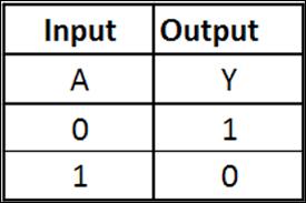
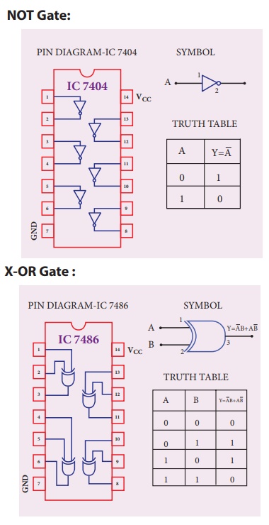
Connection Diagram Function Table Y = A H = HIGH Logic Level L = LOW Logic Level Order Number Package Number Package Description DM7404M M14A 14-Lead Small Outline Integrated Circuit (SOIC), JEDEC MS-012, 0.150 Narrow DM7404N N14A 14-Lead Plastic Dual-In-Line Package (PDIP), JEDEC MS-001, 0.300 Wide Inputs Output AY LH HL Mar 26, 2020 - IC 7400 is fourteen pin Logic Gate IC. The IC 7400 consist of four NAND Gates. Pin diagram of IC 7400 explained here. Operating Condition and Electrical Characteristics of IC 7400 described here. The Internal Structure and Pin Description of IC 7400 explained detail. Application of IC 7400 given here.
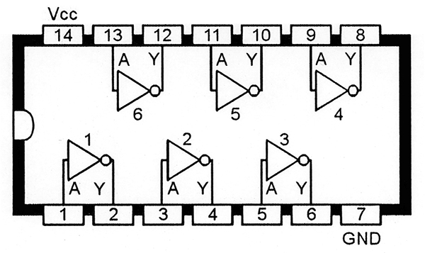
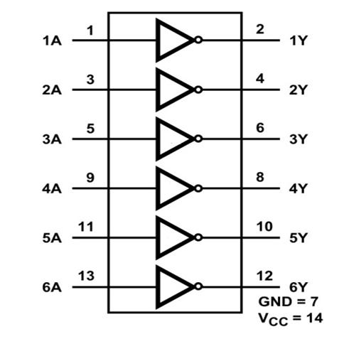
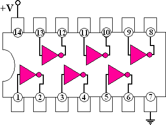
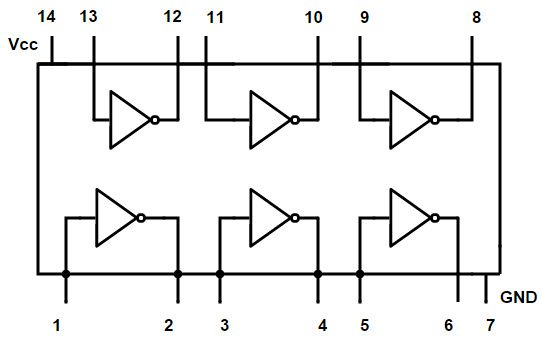
Pin-out diagram of 7404 NOT gate IC. Each 7404 NOT gate IC has 6 NOT gates arranged as shown in the following figure. 14th pin is the Vcc and the 7th pin is the Ground. The outputs directly interface to CMOS, NMOS and TTL. It supports wide operating conditions and has large operating voltage range.
7404 pin diagram
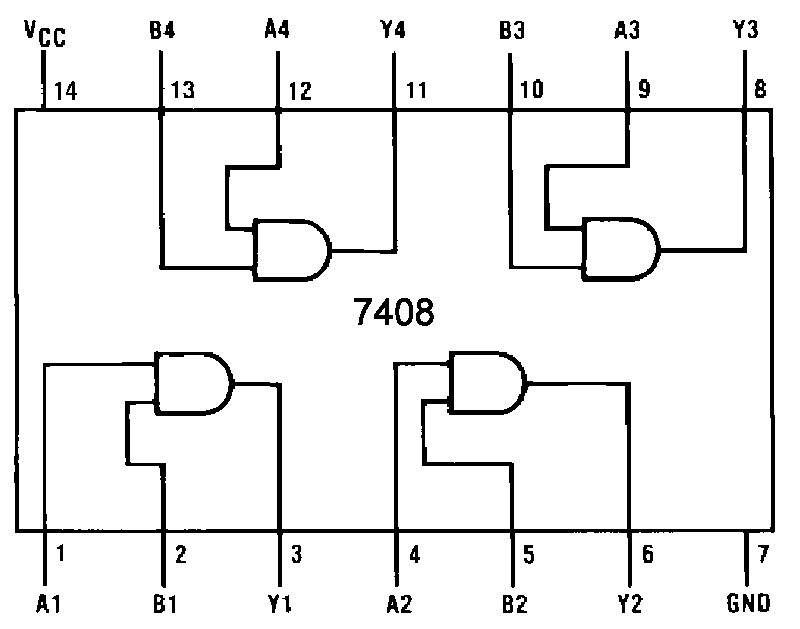
IC 7408 is a logic gate IC. It consists of four two-input AND Gates. The IC 7408 has total fourteen pins including ground and Vcc. The simple pin diagram is shown here. The internal structure of IC 7408 described here. Pin Description of IC 7408 explained in detail. Application of IC 7408 given here. PIN configuration diagram 7 X-NOR GATE. INPUT 3 of GATE 1. PIN configuration diagram 4 NOR GATE. The following logic gate ICs are used in the construction of the circuits 7408 IC The 7408 IC has quad 2-input AND gates. 74LS04 is a14 PIN IC as shown in the 74LS04 pinout. PIN configuration diagram 5 NAND GATE. IC 7400, 7408, 7432, 7447, 7404. Ø IC 7400. IC TTL Seri 7400 adalah kumpulan IC-IC yang turut berperan penting dalam sejarah IC dan penyebarannya. Walaupun telah beredar cukup lama, namun versi-versi modern dari Seri 7400 ini tetap masih digunakan hingga sekarang ini. Pada awalnya, seri 7400 dibuat dengan Transistor bipolar.
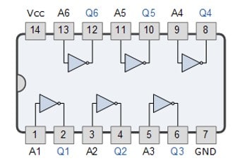
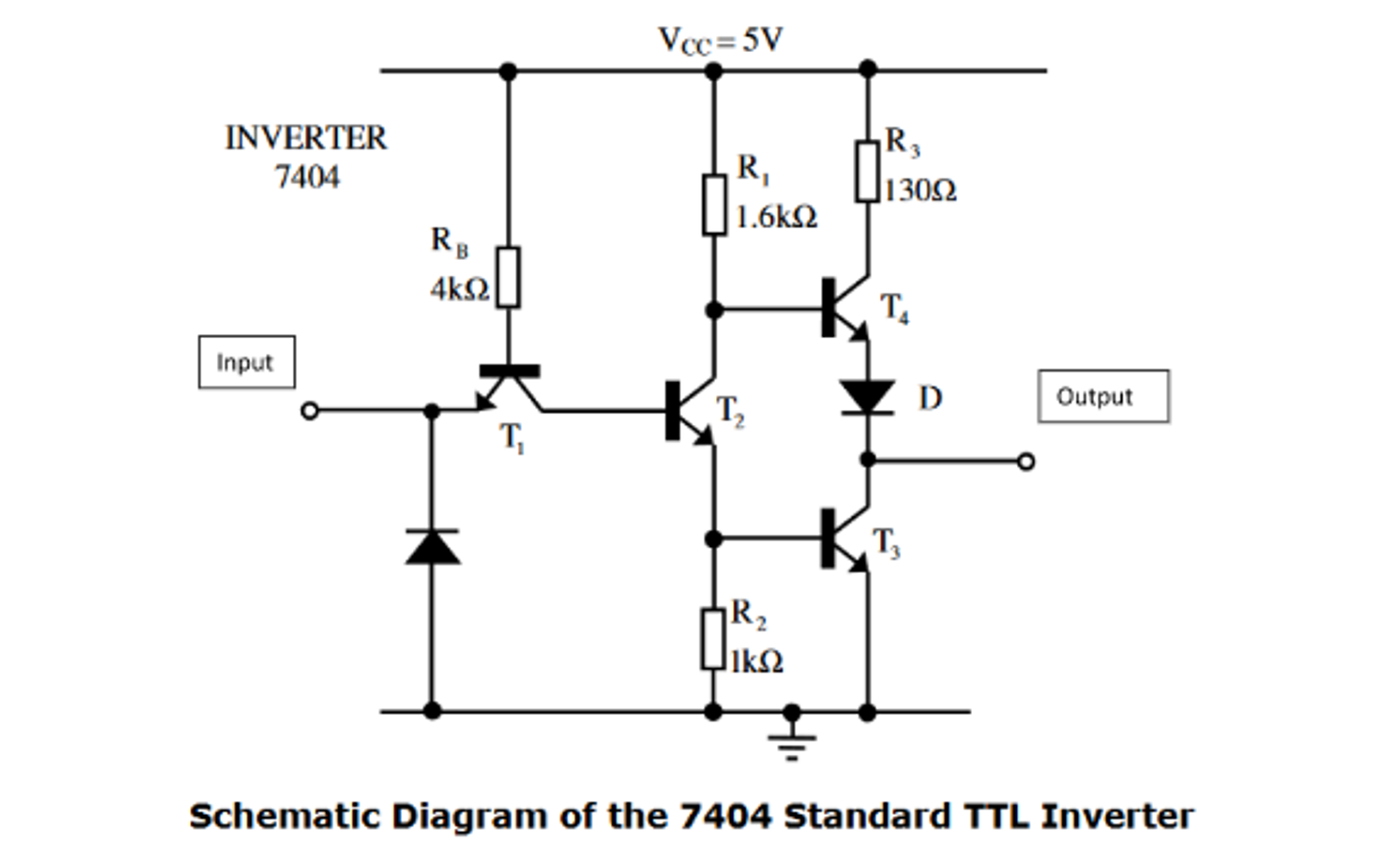
7404 pin diagram. Different types and Study Of Logic Gates: #1. AND Gate: The AND Gate performs the logical multiplication operation which is commonly known as AND function. # If both the inputs are high then the output is high. # If any one of the input is Low then the Output is Low. The IC used for used for AND gate is IC 7408. A two-level logic diagram may be obtained directly from the Boolean expressions derived by the maps. These are various other possibilities for a logic diagram that implements this circuit. Now the OR gate whose output is C+D has been used to implement partially each of three outputs. LOGIC DIAGRAM: (a) Pin diagram for a 7432 IC (b) Pin diagram for a 7404 IC Fig. 6.5 The 7404 IC shown in Fig. 6.5b is also a TTL device. The 7404 IC contains six NOT gates, or inverters. The 7404 is described by the manufacturer as a hex inverter IC. Note that each IC has its power connections (V CC and GND). A 5-V dc power supply is always used with TTL ... 7404, 7404 Datasheet, 7404 Hex Inverter, buy 7404, ic 7404. ... Pin Number Description 1 A Input Gate 1 2 Y Output Gate 1 3 A Input Gate 2 4 Y Output Gate 2 5 A Input Gate 3 6 Y Output Gate 3 7 ...
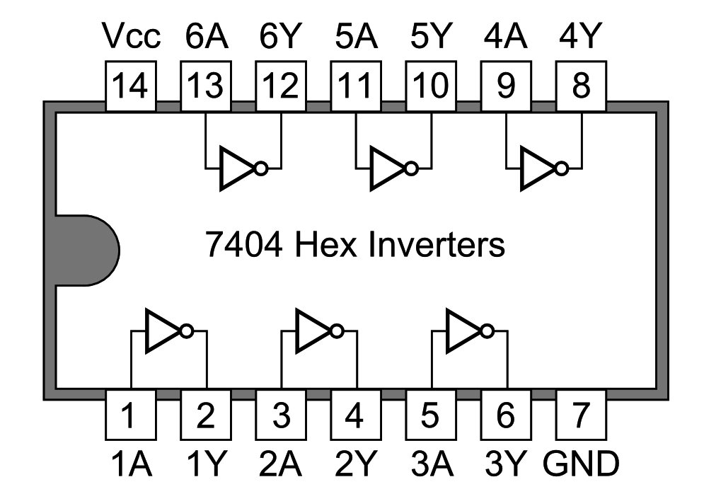
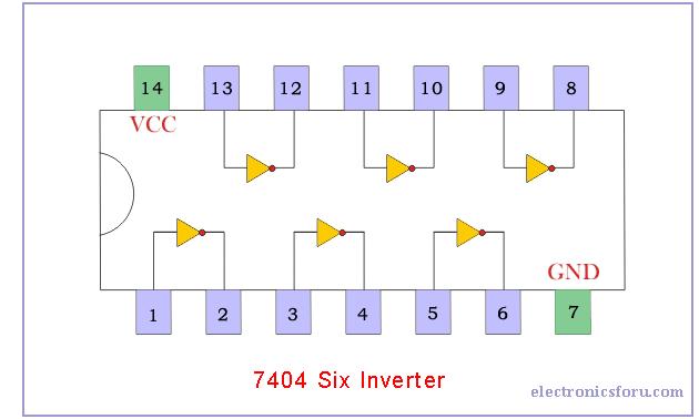
Transcribed image text: 1 Introduction This experiment examines the effect of propagating a signal through multiple gates, using a 7404 hex inverter IC, with pin diagram shown on the back. 2 Propagation Delay 1. The task here is to find an average propagation delay per inverter. (a) Connect the six inverters of the 7404 IC in cascade (the output of one to the input of the next). It is a logical family consisting completely of transistors. It employs a transistor with multiple emitters. Commercially it starts with the 74 series like the 7404, 74S86, etc. It was built in 1961 by James L Bui and commercially used in logic design in 1963. TTLs are classified based … The IC 7400 is a 14-pin chip and it includes four 2-input NAND gates. Every gate utilizes 2-input pins & 1-output pin, by the remaining 2-pins being power & ground. This chip was made with different packages like surface mount and through-hole which includes ceramic (or) plastic dual-in-line and flat pack. ic- 7400 IC 7400 Pin Configuration The 7404 14-pin chip has 6 or hex, inverters. The input and output connections of each of the 6 NOT gates are shown. ... Elevator State Diagram, State Table, Input and Output Signals, Input Latches ; Traffic Signal Control System: Switching of Traffic Lights, Inputs and Outputs, State Machine ...
PIN DIAGRAM: G. PIN DIAGRAM OF IC 7404. HEX NOT GATE. Quad 2-in. puts NOR GATE . G. PIN DIAGRAM OF IC 7447 . BCD TO 7 SEGMENT DISPLAY DRIVER. The appropriate . outputs a-g. become low to display the BCD (binary coded decimal) number supplied on . inputs A-D. The 7447 has . open collector. outputs a-g which can sink up to 40mA. Jun 17, 2015 · Logic gates are the basic building blocks of digital logic circuits as well as digital electronics. A gate is defined as a logic device which computes functionally on a 2 valued input signal. Logic gates are of many types such as OR, AND, NOR, NAND, EX –OR and NOT etc. Among these, all … Jun 20, 2021 · IC 7404 pinout. The IC 7404 is used in different settings as shown above. It also comes in a variety of packages best suited for each application area. The specific applications thus call for the selection of the right package. The description of each gate can be seen from the 7404 pin diagram. You can see 7404 chip pinout diagram image below. What is 7404 chip Pinout diagram? The description of each gate can be seen from the 7404 pin diagram. You can see 7404 chip pinout diagram image below. The IC 7404 is part of a selection of chips that can be configured to form a NOT gate. The 7404 is part of a 74XXX series of chips that are made for a variety of applications.
Understanding Digital Buffer Gate And Logic Ic Circuits Part 2 Nuts Volts Magazine
Aug 29, 2015 · The pin configuration of Hex Inverter 7404 is shown below. Circuit Diagram of Automatic Plant Irrigation System: Circuit Explanation: We are all well aware that the plants will die due to lack of water in the soil. Soil will have high resistance when it is dry and it will have very low resistance when soil is wet. We use this simple logic to ...

Wiring And Testing A 7404 Not Gate Inverter Youtube
7404 Tape and reel SN7404DR SOIC − D Tube SN74LS04D LS04 0°C to 70°C Tape and reel SN74LS04DR Tube SN74S04D S04 Tape and reel SN74S04DR Tape and reel SN7404NSR SN7404 SOP − NS Tape and reel SN74LS04NSR 74LS04 ... logic diagram (positive logic) 1A 2A 3A 4A 5A 6A 1Y 2Y 3Y 4Y 5Y 6Y Y = A

Pin On Electronics
74LS04 Pin Digram. This a pinout diagram of hex NOT gate 74LS04IC.. Other logical gates: 74LS138, 74LS00, 74LS02 74LS04 IC PIN CONFIGURATION Details This table lists 74ls04 NOT gate details of all pins.
Ic 7404 Datasheet And Pinout Hex Inverter Chip Netsonic
7404 IC - The 7404 IC has six inverting gates. The IC has the following pin configuration - Fig. 8: Table listing pin configuration of 7404 IC. The IC has the following Pin Diagram - Fig. 9: Pin Diagram of 7404 IC. The IC requires a supply voltage of 5V which can be tolerated up to 7V.

File 7404 Hex Inverters Png Wikimedia Commons
PIN configuration diagram 5 NAND GATE. Circuit diagram and working of NAND gate. PIN Configuration diagram of Logic Gates 1 NOT GATE. The IC 7400 consist of four NAND Gates. Any of the two chips can be. The IC requires a supply voltage of 5V which can be tolerated up to 7V. Pin 7 is the ground pin that provides power to the chip.

Pin Rearrangements Of Gates 7400 7402 7404 7408 And 7432 And Gate Download Scientific Diagram
74LS02 Quadruple 2-Input NOR Gate IC. 74LS IC series comes up with multiple gates. It provides us with compact design and multiple packages of the same IC. Here we will discuss 74LS02. 74LS02 also know as 7402. IT comes up with 4 internal NOR gate. IC 7402 comes up in multiple packages with 14 pins and 2 inputs 4-NOR gates. NOR gate is designed ...

Pin Rearrangements Of Gates 7400 7402 7404 7408 And 7432 And Gate Download Scientific Diagram
IC 7483, IC 7404, etc. Procedure: - 1. Apply the inputs to A0 to A3 and B0 to B3. 2. Connect C0 to the Ground. 3. Check the output sum on the S0 to S3 and also C4. 4. For subtraction connect C0 to Vcc, Apply the B input through NOT gate, which gives the complement of B. 5. The truth table of adder and Subtractor are noted down. Truth Table for ...
Get Started With Not Gate Ic 7400 Series Tutorial
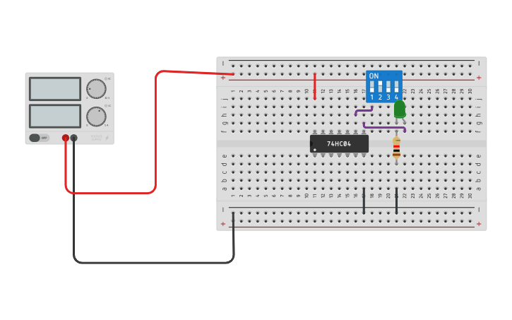
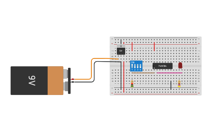
We have already seen, controlling 7404 using switch. Controlling 7404 using Arduino is more simple. Circuit is done as shown in the following diagram. An arduino mega is used to control 7404. 5V for IC is supplied from the 5V pin of Arduino Mega. Ground is given to the, GND pin of Arduino.
1
8085 Pin Diagram TDA7273 TDA7274 L6219 UDx2916 L293 LMD18200 SN754410 AD9573 AAT3128 TB2901H TDA1301 TDA1085CD TDA10046 DVB T-Channel Receiver TD7626F,TD7626FN 4N25 16f84 ... 7404 7430 7421 7420 7427 7412 7411 7410 74132 7486 7432 7409 7408 7403 7402 7400 4000 Series CMOS IC Info 317 topics total. 7408. 7408
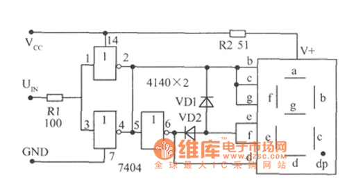
The Level Test Circuit Diagram Composed Of 7404 Ttl Hex Not Gate Measuring And Test Circuit Circuit Diagram Seekic Com
7404 IC - The 7404 IC has six inverting gates. The IC has the following pin configuration - The IC has the following Pin Diagram - Fig. 8: 7404 Pin Diagram. The IC requires a supply voltage of 5V which can be tolerated up to 7V. The voltage at the inputs of NOT gates must be 2V for high logic and 0.8 V for low logic.
74ls04 Pinout Features Equivalent Examples Datasheet
Jun 01, 2018 · Logi7400. Logisim 7400 series integrated circuits library.. Variants. There are two variants of the library with different circuit appearances available: In the classic Logi7400dip library, the circuit appearance reflects the physical pin layout of the DIP packaged chips.; The new Logi7400ic library provides a logical circuit appearance.; Goal. This library aims to be a comprehensive 7400 ...
What Is Not Gate Inverter Not Logic Gate Inverter Circuit Using Transistor
14+ 7448 Ic Pin Diagram. Ic 74hc08, ic dm7408 are and gate ics. Once the lamps are ignited and the voltage at isen (pin 14) is > 0.7v, the ic enters the normal operation mode and the pwm dimming. This video shows you how to use the 7 segment display (common cathode means postive) with the help of 7447 ic. It is a video on basic explanation of ...
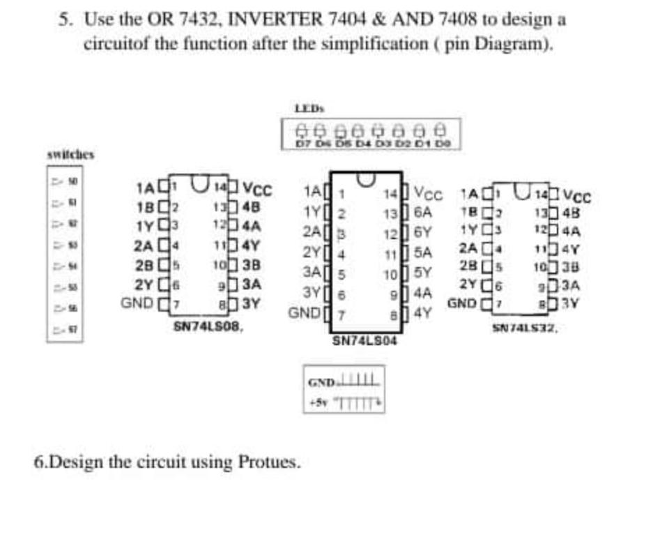
5 Use The Or 7432 Inverter 7404 And 7408 To Chegg Com
IC 7404 or IC 74LS04 is a logic gate IC. It consists of six NOT Gates. The IC 7404 consists of fourteen pins each pin are shown here. Know about operating condition and characteristics of IC 7404. Internal structure and pin description of ic 7404 is given here. Read all the applications of IC 7404 here.
Circuit Diagram Of Ic 7404 Ebooks And Journals
7400,7402,7404,7408,7432,7486 ICs pin diagrams
Digital Circuits For High School Students Part 1
III. Connect the wire to the main voltage source (Vcc) whose other end is connected to last pin of the IC (14 place from the notch). IV. Connect the ground of IC (7th place from the notch) to the ground terminal provided on the digital lab kit. V. Give the input at any one of the gate of the ICs i.e. 1st, 2nd, 3rd, 4th gate by using connecting ...
7404 Hex Inverter
13+ Ic 7432 Pin Diagram. Pin diagram of 7404 ic. Here xor gate ic 7486 and logic and gate ic 7408 and or gate ic 7432 are used to construct the full adder circuit, both are quad 2 input logic gate ic. To understand the digital system or circuit we should understand the logic gates and it's input/output behavior properly.

Logic Gate Implementation Of Arithmetic Circuits De Part 11
Pinout diagram of 7404 is given below. Each 7404 has 6 NOT gates arranged as shown in the following figure. 14th pin is the Vcc and 7th pin is the Ground. Recommended operating conditions of 7404
7404 Not Gate
IC 7400, 7408, 7432, 7447, 7404. Ø IC 7400. IC TTL Seri 7400 adalah kumpulan IC-IC yang turut berperan penting dalam sejarah IC dan penyebarannya. Walaupun telah beredar cukup lama, namun versi-versi modern dari Seri 7400 ini tetap masih digunakan hingga sekarang ini. Pada awalnya, seri 7400 dibuat dengan Transistor bipolar.
Get Started With Not Gate Ic 7400 Series Tutorial
PIN configuration diagram 7 X-NOR GATE. INPUT 3 of GATE 1. PIN configuration diagram 4 NOR GATE. The following logic gate ICs are used in the construction of the circuits 7408 IC The 7408 IC has quad 2-input AND gates. 74LS04 is a14 PIN IC as shown in the 74LS04 pinout. PIN configuration diagram 5 NAND GATE.
Ic 7404 Not Gate Tinkercad
IC 7408 is a logic gate IC. It consists of four two-input AND Gates. The IC 7408 has total fourteen pins including ground and Vcc. The simple pin diagram is shown here. The internal structure of IC 7408 described here. Pin Description of IC 7408 explained in detail. Application of IC 7408 given here.

Electronics 7404
7408

Pin On Electronics

Control 7404 Not Gate Ic Using Arduino Mega Funny Electronics
Solved 1 What Are Input And Output Voltages For This Chegg Com
Verification Of Truth Tables Of Logic Gates Using Integrated Circuits Physics Practical Experiment

Simple Electronic Circuit Water Level Indicator Using 7 Segment Display This Water Level Indicator Uses A 7 Segment Display Instead Of Leds To Indicate The Water Level Low Half And Full In The Tank

Ic 7404 Pin Diagram Circuit Design Data Sheet Application Etechnog

7404 Datasheet Stmicroelectronics Datasheetspdf Com

7404 Pinout Android Touch Screen Bathroom Towel Decor

7404 Datasheet
Digital Logic Not Gate
Combinational Logic Circuit Using 7404 7408 7432 Tinkercad

Logic Gate Ic S Concise Information And Various Applications Of Logic Gate Ic S
Pg1n S Ham Radio Site Ic 74xx Serie 7404
Digital Electronics Circuit In Breadboard Not Inverter Logic Gate Ic 7404 And Truth Table Youtube

Control 7404 Not Gate Ic Using Switch Funny Electronics
Digital Circuits For High School Students Part 1
Comments
Post a Comment